Author : Daeguen Lee (DGLee)
Contact : leedaeguen [at] kaist.ac.kr
(Any action violating either CCL policy or copyright laws is strictly prohibited)
엔비디아 지포스 GTX 750 Ti (맥스웰) 리뷰

Introduction
2010년의 페르미, 2012년의 케플러에 이어 만 2년만에 엔비디아의 새 아키텍처 "맥스웰"이 모습을 드러냈습니다.
다만... 많은 사람들이 기대했듯 GK110의 뒤를 잇는 차세대 플래그십을 통해 소개된 것은 아니고, 엔트리 레벨에 해당하는 GM107 GPU를 적용한 GTX 750 / GTX 750 Ti가 맥스웰 패밀리의 첫 타자로서 타석에 서게 되었습니다. 이들은 각각 시장에서 GTX 650 / 650 Ti의 뒤를 이을 예정이며, 특히 GTX 650과는 다르게 상위 GPU의 컷팅 버전이었던 GTX 650 Ti와 달리 GTX 750 Ti는 태생부터 GTX 750과 같은, (아마도 맥스웰 패밀리 중 가장 작은 GPU일) GM107을 탑재하고 있어 제조사의 입장에서는 원가절감이라는 측면에서 가장 큰 기대를 걸 법한 제품이기도 합니다.
엠바고가 풀리기 한참 전부터 GM107의 스펙과 성능에 관해 많은 루머들이 돌아다닌 바 있습니다. 과연 그 실체는 어떠할지, 리뷰를 통해 알아봅시다.
Today, NVIDIA introduced its next-generation graphics architecture "Maxwell", first as a replacement of entry-level product of current generation, GK107 based on Kepler architecture, namely GM107. (M in its codename refers Maxwell as well as K in GK107 means Kepler) Recently (for more than a couple of years) NVIDIA has launched its new architecture every even year, for example, Tesla for 2008, Fermi for 2010 and Kepler for 2012, and this biennial rule made it more predictable that the company will release post-Kepler product sooner or later. Many enthusiasts have been questioning how fast the new flagship GPU compared to GK110. This question may, however, not be answered today. Since today we only got a baby Maxwell.
In fact, release of GM107 is not that typical though the biennial rule is held, since on the other hand the company's product differentiation strategy goes somewhat differently than previous generations : GM107 itself is the symbol of NVIDIA's first bottom-up approach within a generation thank to delay of 20nm fabrication process by TSMC. In 2008, NVIDIA launched GTX 260/280 based on GT200 GPU, the biggest silicon ever made upon Tesla architecture, as the first Tesla chip at the same time. Smaller variations such as GT215/GT218 appeared a year later than GT200. In Fermi era, the same footage is repeated : GF100 -> GF104 -> GF106/108. These all can be categorized as top-down approaches. What made this kind of approach actually works is evolution of fabrication process. 55nm process was matured when Tesla was introduced as well as 40nm was matured when Fermi came, so was 28nm for Kepler. For Maxwell, however, there was no matured 20nm fabrication process and thus making a big chip based on Maxwell is virtually impossible as of today. This is why NVIDIA changed its differentiation strategy from top-down to bottom-up.

엔비디아는 맥스웰 아키텍처의 특징을 수많은 미사여구를 동원해 설명하고 있지만 핵심은 아래의 두 문장으로 요약됩니다.
1. 하나의 SM 단위 (맥스웰의 SMM, 케플러의 SMX) 를 비교했을 때 케플러의 90% 성능을 내면서 면적은 그보다 훨씬 작아졌다고 합니다. 192SP/16TMU -> 128SP/8TMU가 되었음을 생각하면 당연한 결과입니다 즉 단위 SM 성능 자체는 케플러보다 떨어졌지만 SMM 자체의 면적이 크게 줄어 더 많은 수를 탑재할 수 있게 되었다는 것인데, 실제로 GM107은 5개의 SMM을 탑재하고 있으며 이는 GK107의 2 SMX / GK106의 4 SMX보다 더 많은 수임을 상기하시기 바랍니다. 아주 단순히 계산해서, GK106의 성능을 400%라 두면 GM107은 90% x 5 = 450%로 GM106보다 더 높은 성능을 낼 수 있을 것처럼 여겨지기도 합니다. 물론 이렇게 계산이 쉽게 될 리는 없고 -_-; 최소한 GK107보다는 크게 향상된 성능을 기대할 수 있겠죠.
2. 에너지 효율을 따졌을 때 케플러의 두 배, 페르미의 네 배가 되었다고 합니다. (정확히는, 비교 대상은 GTX 550 Ti -> 650 Ti -> 750 Ti라고 합니다) 아키텍처가 변화함에 따라 전력 효율이 달라지는 것은 늘 있어 왔던 일인데, 이번에는 L2 캐시가 256KB에서 2MB로 는 것이 코어의 효율 향상에 큰 도움이 되었다고 합니다. (늘어난 캐시로 인해 메모리 대역에의 의존도가 줄었다고도 합니다) 그간 GPU의 성능 향상은 연산유닛 자체를 증가시키는 데 매달려 왔지만 이런 방식의 접근은 과거 CPU 제조사들이 CPU 성능을 향상시키기 위해 자주 써 온 기법이란 점에서, 새삼 GPU의 CPU화가 와닿는군요.
As a first Maxwell variant, GM107 features followings :
- Different core config : 192 CUDA / 16 TMU per SMX -> 128 / 8 per Maxwell SM (SMM)
- Higher energy & performance efficiency, mainly derived from smaller SM design
- Less susceptible to graphics memory bandwidth thank to enlarged L2 cache : 256KB -> 2048KB
Many of above are highly anticipated that we can see them in bigger Maxwell as well. For short, Maxwell features "(relatively) smaller die size, higher efficiency" in compared to Kepler. Well, let's taste these out by testing our very first GM107 SKU, GeForce GTX 750 Ti.
Test Setup & Methodology
테스트에 사용된 시스템 사양은 아래와 같습니다.
Test system I used consists as follow.

테스트 방법은 그동안과 같이, 각 게임별/해상도별로 3회 반복 테스트 수행 후 중간값을 결과값으로 취했습니다. 각 게임별로 그래픽 품질은 게임 내에서 설정 가능한 최상위 옵션으로 설정하였으며 (= 풀옵), 다만 안티알리아싱은 적용하지 않는 것을 원칙으로 했습니다. 자세한 옵션 세팅에 관해서는 각 게임별 결과를 소개해드리는 장에서 따로 언급하도록 하겠습니다.
I ran all games 3 times repeatedly for each resolution and choose the median as the represent value for the game under each resolution. Graphics quality of each game was the highest possible in-game settings except anti-aliasing. Further details will be noted in test result chapters.
In-Depth Analysis on Maxwell
본격적으로 벤치마크를 시작하기 전에, 먼저 맥스웰 아키텍처를 대략적으로 살펴보도록 합시다.
우선 GM107과 직접적으로 비교 가능한 GPU는 GK107과 GK106 두 가지인데, 이들 GPU를 사용한 대조군들을 비교해 보도록 하겠습니다.
Before we go for tests, I want to give you some theoretical backgrounds. Let's see this table.

보시다시피 GM107의 스펙은 GK106과 GK107의 정 가운데쯤에 위치합니다. 쿠다코어 갯수는 둘 중 GK106에 더 가까우나 쿠다코어 대비 TMU 비율이 크게 떨어져 (케플러의 경우 12:1, 맥스웰은 16:1) TMU, ROP 등은 오히려 GK107에 더 가까운 모습을 보이고 있습니다. 물론 아키텍처가 바뀐 만큼 개별 쿠다코어 갯수, 개별 TMU 갯수를 일대일로 비교할 수 없음을 감안하면 이 시점에서 성능 계산은 어렵겠지만, 어쨌든 내부적으로 각 유닛들의 구성비가 변화한 만큼 내부 구조 역시 상당히 달라졌을 것이란 추측이 가능합니다. 이에 관해 엔비디아가 제공한 블록 다이어그램은 아래와 같습니다.
GM107 seems lie between GK106 and GK107 in terms of its backend units : CUDA core count is more like GK106 than GK107 while the contrary is more likely for anything other than CUDA - TMU count, ROP count and memory interface of GM107 is more like GK107 than GK106. Based on that, GM107 is expected to perform 'a bit' faster than GK107 and 'a double bit' slower than GK106 if there is no architectural change in sub-SM unit level. In other words, If actual GM107 (GTX 750 Ti) would performs better than provided below, it means there are some primitive improvements in Maxwell architecture. See below.

The table is derived by VGA calculator I designed. By assuming that all units among SKUs are vertically equivalent(that is, 1 CUDA core of GTX 650 Ti is same as 1 CUDA core of GTX 660, 1 TMU of GTX 650 Ti is same as 1 TMU of GTX 660, and so on), 'conceptual' GTX 750 Ti will have overall performance just one-digit % faster than GTX 650 Ti and about 30% slower than GTX 650 Ti Boost. Let's keep that in mind and compare the virtual results derived in Performance Summary chapter. Then we know whether Maxwell can be distinguishable from Kepler or not.
(※ To know more about "VGA calculator", see this : -link-)
A Closer Look : The Card
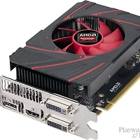
오늘의 주인공, 지포스 GTX 750 Ti의 사진들입니다.
There are some images of GTX 750 Ti.


Result : 1. 3DMark 11
(Entry / Performance Preset)


2. 3DMark 2013
(Cloud Gate / Fire Strike)


3. Alan Wake
(All High, AA 2x, FXAA Off)


4. Aliens vs Predator
(Texture : Very High, Shadow : High, AF 16x, SSAO/Tessellation/Advanced Shadow On, AA Off)


5. Batman : Arkham City
(DX11 Features : MVSS and HBAO, DX11 Tessellation : High, Detail Level : Extreme, AA/PhysX Off)


6. Battlefield 4
(Ultra Preset, Deferred AA Off)


7. Bioshock : Infinite
(UltraDX11 with Diffusion Depth of Field)


8. Borderlands 2
(Texture/Detail : High, Decal : Very High, SSAO/DOF On, AF 16x, FXAA/PhysX Off)


9. Call of Duty : Ghosts
(Image/Texture/Terrain : Extra, DOF/Shadow On, SSAO/AF : High, AA/Fur Off)


10. Company of Heroes 2
(Image Quality : Maximum, Texture : Higher, Snow/Physics : High, AA Off)


11. Crysis : Warhead
(64bit, DX10, Enthusiast, AA Off)


12. Crysis 3
(Texture Resolution/System Spec : Very High, AA Off)


13. DiRT : Showdown
(Ultra Preset, AA Off)


14. Hitman : Absolution
(Quality Level : Ultra, AA/FXAA Off)


15. Just Cause 2
(Texture/Shadow/SSAO : High, Water/Objects : Very High, All others On except AA)


16. Lost Planet 2
(All High, AA Off)


17. Metro 2033
(DX11, DOF On, Quality : Very High, AF 16x, AA/PhysX Off)


18. Metro : Last Light
(DX11, Quality/Tessellation : Very High, AF 16x, AA/PhysX Off)


19. Resident Evil 6
(Shadow/Texture/Screen : High, AA Off)


20. Sleeping Dogs
(Graphics Level : Extreme, AA : Normal)


21. Splinter Cell : Black List
(Graphics Quality : Ultra, AA Off)


22. Tomb Raider : Reboot
(Quality : Ultra, AA Off)


Performance Summary
코멘트 한줄 없이 수백여장의 그래프를 보시느라 수고 많으셨습니다.
Congratulations for not drowned by graphs. They are all finished - except three below.


종합적으로, GTX 750 Ti는 (비슷한 이름에서 유추할 수 있듯) 시장에서 그 자리를 대체하게 될 GTX 650 Ti보다 25%가량 더 빠르고, 엔비디아의 팹 전략상 같은 위상을 갖는 GK107 기반의 GTX 650보다는 거의 두배 가까이 빠른 성능을 보입니다. 한편 GK106 기반의 GTX 660, GTX 650 Ti Boost보다는 분명히 느린 성능을 보이며 GTX 650 Ti Boost와의 차이는 약 6% 정도입니다. 라데온들과 비교하자면 GTX 750 Ti는 R7 260X와 7850의 정확히 한가운데쯤에 해당하는 성능을 보입니다. 한편 GTX 750 Ti의 가격은 150달러로 예고되어 있는데, 이는 현존하는 동가격대 그래픽카드들과 비교해 딱히 나쁘거나 딱히 더 좋지 않은, 정확히 그 성능을 반영한 가격대로 보여집니다.
As a whole, GTX 750 Ti is about a quarter % faster than GTX 650 Ti, almost twice than GTX 650 and 6% slower than GTX 650 Ti Boost. In comparison with Radeon counterparts, GTX 750 Ti lies almost at the middle between Radeon R7 260X and 7850. When it comes to a matter of actually "buy" a graphics card, one we must consider is performance-per-price. GTX 750 Ti is announced as $150, a price that almost exactly represent its relative performance among current generation competitors - Nothing blazingly good, nothing bad.
Conclusion
지금까지 GTX 750 Ti의 모든 테스트 결과와 종합 성능을 살펴보았습니다. 여러분이 생각하시기에, GTX 750 Ti가 괜찮은 제품 같아 보이시는지요.
개인적으로는 현존하는 자사 구세대 및 경쟁사의 라인업이 이미 형성한 가격-성능 질서 안에서 GTX 750 Ti의 위치를 억지로 찾아내는 것보다 더 중요한 함의가 GTX 750 Ti에게 있다고 생각합니다. 그것은 바로 이 제품이 '첫 번째 맥스웰' 이라는 점에 있습니다.
하지만 중요한 것은 가격 그 자체보다도, 출시 이후 시장의 수요-공급 원리에 따라 결정되는 "실 거래가" 아니겠습니까. 비트코인이든 라이트코인이든, 어떤 요인으로든 현재 AMD는 자사 그래픽카드의 수요를 따라잡지 못해 지속적인 가격 상승을 사실상 방치하고 있는 상황이며 단지 현존하는 7850을 R7 265라는 이름으로 바꿔, 낮은 가격표를 붙여 출시한다고 하여 갑자기 대량생산이 가능해지게 될 것이라 믿을 어떤 이유도 없기에 진정 가성비 왕으로 등극하기 위해서는 넘어야 할 산이 많아 보입니다. 물론 이 모든 회의적인 시각을 뒤로 하고, 표면적으로 드러난 정보들로만 판단하자면 R7 265는 현 세대에서, 그리고 그 가격대에서 가장 매력적인 제품 중 하나임에는 틀림이 없습니다. 결국 문제는 아주 기본적인 경제학 원리로 환원되는군요. "수요와 공급"
GTX 750 Ti, 아니 GM107은 맥스웰 아키텍처가 적용된 첫 번째 GPU로써 GK107보다는 66% 더 많은 쿠다코어 / 25% 더 많은 TMU / 동수의 ROP, 메모리 인터페이스를 가집니다. 물론 내부적으로는 '듀얼코어' 와 '5코어' 만큼의 간극이 있어 절대 일대일 비교는 불가능하나, 분명한 것은 스펙상의 증분(increment)이 종합적으로 +50%가 될까말까한 상황에서 거의 GTX 650 대비 두배 가까운 성능향상을 보였다는 점입니다. 분명히 엔비디아는 개별 유닛 차원에서 효율성을 증대하는 데 성공한 것 같습니다.
GK106과 비교했을 때 GM107은 TMU는 1/2 수준에 불과한데다 쿠다코어/ROP/메모리 인터페이스는 2/3 수준에 그칩니다. 그럼에도 불구하고 GTX 650 Ti Boost와는 사실상 동등한 성능을, GTX 660과 비교해도 80%를 상회하는 수준의 성능을 달성했다는 것은 앞서 GK107과의 비교에서 도출한 결론인 "개별 유닛의 효율이 증대되었다" 는 명제의 설득력을 다시 한번 높여 주고 있습니다. 여기서 잠시 2페이지의 스펙 비교표를 되새겨보면 GM107은 148 제곱밀리미터의 면적만으로 118 제곱밀리미터의 GK107의 두배 가까운 성능을, 221 제곱밀리미터의 GK106의 80%에 해당하는 성능을 발휘하고 있는 셈입니다. 맥스웰의 진가는 이 대목에서 찾아야 하지 않을까요.
종합하자면, GTX 750 Ti 자체는 GTX 650 Ti Boost와 동급으로 (미세하게나마 모든 해상도에서 더 낮은 성능이긴 합니다) 딱 예상되었던 바 그대로의 성능을 보였으며, 일단 이 제품 하나로 전체 시장이 교란되거나 라인업의 창조적 파괴가 이뤄질 정도의 잠재력은 없다고 생각됩니다. (가격이 $70 <- 뭐 이런식으로 매겨지지 않는 한 -_-;) 가격대가 GTX 650 Ti Boost와 비슷하다면 여전히 라데온 7850이 더 매력적인 가성비를 제공하는 옵션으로 남으며, 며칠 전 출시된 R7 265 역시 GTX 750 Ti와 같은 가격대로 매겨진 반면 성능은 한급 위인 GTX 660과 엎치락뒤치락 하는 수준입니다. 하지만 GM107이 보여준 맥스웰의 잠재력은 결코 무시할 수 없습니다.
GM107의 면적대비 성능이 고스란히 구현된, 지금의 GK110 정도 면적의 빅 칩이 출시된다면...?
오늘만큼은 제품에 대한 판단뿐 아니라, 독자 여러분께 상상의 여지까지 한 꼭지 남겨드린 채 글을 맺을까 합니다.
긴 글 읽어주셔서 감사합니다 :-)
So far we have covered how fast (or slow) GTX 750 Ti is. Do you think it's an attractive newbie on graphics card market? To answer this question, we must distinguish the GM107 itself and GM107-based SKU, GeForce GTX 750 Ti. Let's first discuss about the latter.

Despite the fact that nomenclature of GTX 750 Ti resembles that of GTX 650 Ti and GTX 750 Ti is significantly faster (+25%) than its predecessor, GTX 750 Ti itself is not an eye-popping attractive product in terms of performance. It just lies between GTX 650 Ti and GTX 650 Ti Boost, both of them are currently tangible & affordable. In other words, GTX 750 Ti throws nothing special in that price-performance niche in graphics card market : existing-level performance for existing-level perf/price ratio. Does is make sense?
When we talk about the former, however, the tone must be changed. As the first tangible silicon based on Maxwell architecture, GM107 features 66% more CUDA cores than GK107, 25% more TMUs and same amount of ROPs as well as same memory interface. Though we cannot compare those units apple-to-apple match, it is possible to be said that GM107 is almost twice faster than GK107 despite the fact that it only earns +0~66% of units in their own kind. Increment on performance definitely excess the increment on backend hardwares. In other words, NVIDIA succeeded to improve unit-level efficiency in Maxwell architecture. In addition to that, Maxwell's silicon efficiency is also impressive. Die area of GM107 is only 148 mm2 (square milimeter) while GK106 is 221 mm2 and GK107 is 118 mm2. Remind that GM107 is as twice faster than GK107 while die area is only bigger by 20% and reaches over 80% of performance of GK106 while GM107 occupies 60% of silicon of GK106.
Just Imagine : "Maxwell's efficiency done within & fully utilized the size of current big chip."
Well, the article is finally over.
Thank you all for reading my words. Have a nice day!
//
(아래 위젯은 티스토리의 크라우드펀딩 시스템인 '밀어주기' 위젯입니다. 100원부터 3000원까지의 범위 내에서 글쓴이에게 소액 기부가 가능합니다. 사견으로는 이러한 형태의 펀딩이야말로, 성공적으로 정착될 경우 이해관계자로부터 독립된 벤치마크가 지속가능해지는 원동력이 될 것이라 생각합니다. 제가 작성한 글이 후원할만한 가치가 있다고 여기신다면 밀어주기를 통한 후원을 부탁드립니다. 물론 글을 '가치있게' 쓰는 것은 오롯이 저의 몫이며, 설령 제 글이 '후원할 만큼 가치있게' 여겨지지는 못해 결과적으로 후원을 받지 못하더라도 그것이 독자 여러분의 잘못이 아니란 건 너무 당연해 굳이 언급할 필요도 없겠습니다. 저는 후원 여부와 관계없이 제 글을 읽어주시는 모든 독자분께 감사합니다.)
'Review > vga_review' 카테고리의 다른 글
| AMD 라데온 R7 250 리뷰 : Best for Kaveri, or not? (0) | 2014.04.03 |
|---|---|
| AMD 라데온 R7 250X 리뷰 : 같은 칩, 다른 이름? (3) | 2014.03.30 |
| AMD 라데온 R7 265 리뷰 (6) | 2014.02.18 |
| 티타늄의 귀환 : 엔비디아 지포스 GTX 780 Ti 리뷰 (12) | 2013.11.07 |
| AMD 라데온 R9 290 (non-X) 리뷰 (3) | 2013.11.05 |